


Look and see
-
¥99999.00
-
¥99999.00
-
¥99999.00
-
¥99999.00
-
¥99999.00
-
¥99999.00
-
¥99999.00
-
¥99999.00
-
¥99999.00
-
¥99999.00
Product Description
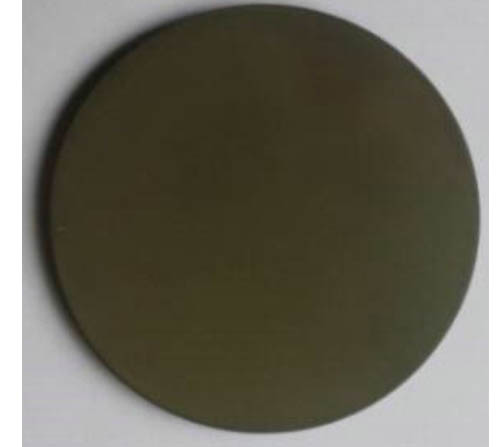
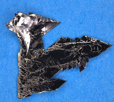
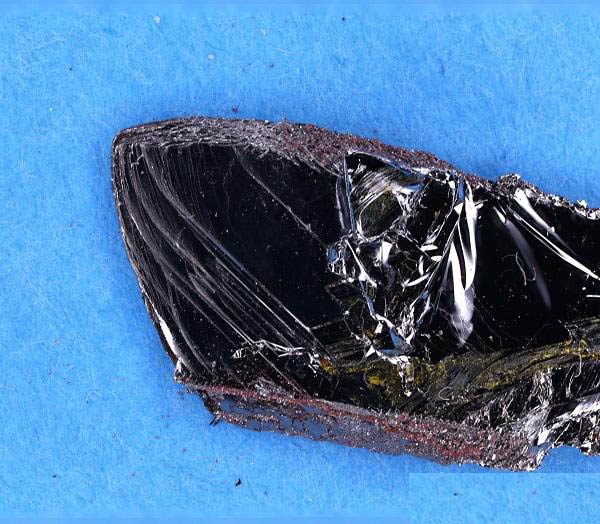
In the bulk form SnSe has band-gap at around 0.9 eV (indirect) and 1.25 direct gaps. It has layered structure (lamellar) with weak interlayer coupling, enabling to isolate down to monolayers. Each monolayer is four atoms thick (Se-Sn-Sn-Se) that is roughly 0.9-1.0 nm. At high pressures it undergo semiconductor to superconductor transition. More recently, SnSe has been shown to display world record performance for thermoelectric material efficiency.
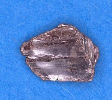
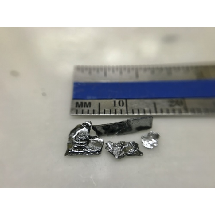
SnSe single crystal characteristics
| Crystal size | 1cm in size |
| Material properties | Thermoelectric semiconductor (anisotropic semiconductor) |
| Crystal structure | Pnma [62] |
| Unit cell parameters | a=0.421nm,b=0452nm, c=1.181nm,α=β=γ=90° |
| Growth method | Bridgman growth technique |
| Purity | 99.9999% confirmed |
Raman spectrum collected from SnSe crystals